
Clamper Circuits
Note: The circuits which are used to add a d.d. level as per the requirements to the a.c. output signal are called calmper circuits.
The capacitor, diode and resistance are the three basic elements of clamber circuit. The clamber circuits are also called d.d.restorer or d.c. inserter circuits.
Depending upon whether the positive d.d. or negative d.d. shift is introduced in the output form,the clambers are called classified as,
a) Negative clambers b) Positive clambers
Let us study these two circuits.
1.1. Negative clamber
A simple negative clamber which adds a negative level to the a.c. output is shown in the Fig 1. It consists of a capacitor C, the ideal diode D and the load resistance RL.
 |
| Fig 1 Negative clamber |
The following assumptions are made analysing the clamber circuit;
1. The diode is ideal in behaviour.
2. The time constant t = RC is designed to be very large by selecting large values of R and C.
Operation :
During the first quarter of positive cycle of the input voltage Vi, the capacitor gets charged through forward biased diode D upto the maximum value Vm of the input signal Vi. The capacitor charging is almost instantaneous, which is possible by selecting proper values of C and RL in the circuit. The capacitor once charged to Vm, acts as a battery voltage Vm as shown in the Fig 2.
 |
| Fig 2 |
Thus when D is ON, the output voltage Vo is zero.As voltage decreases after attaining its maximum values Vm, the capacitor remains charged to Vm and the diode D becomes reverse biased.
Due to large RC time constant the capacitor holds its entire charge and capacitor voltage remains as Vc= Vm as shown in the Fig 3.
 |
| Fig 3 |
And the output voltage Vo is now given by,

Note : This is as good as adding a negative d.c. level equal to -Vm to the output.
In the negative half cycle of Vi, the diode will remains revers biased. The capacitor starts discharging through the resistance RL. As the time constant RLC is very large, it can be approximated the the capacitor holds all its charge and remains charged to Vm, during this period also. Hence we can write again that,

Waveforms :
Assuming ideal diode, the input and output waveforms are shown in the Fig 4.
 |
| Fig 4 negative clamper waveforms |
The peak to peak amplitude of the input is 2Vm,similarly the peak to peak amplitude of the output is also 2Vm. Thus the total swing of the output always same as the total swing of the input, for a clamber circuit.
Square wave input :
If the same clamber circuit is subjected to square wave type input, capacitor charges to peak value of input voltage almost instantaneously and net output in positive half cycle remains zero. In negative half cycle, the output swings to twice the peak value of voltage and remains constant during negative half cycle of the input voltage Vi.
Note : The total swing of the input is same as the total swing of the input.
The Fig 5. shows ther input and output waveforms for square wave input.
 |
| Fig 5 waveforms for square wave input |
1.2 Positive Clamber
The circuit is shown in the Fig 6.
The circuit is shown in the Fig 6.
 |
| Fig 6 positive clamper |
Note : By changing the orientation of the diode in the negative clamber, the positive clamber circuit can be achieved.
Operation : During the first quarter of negative half cycle of the input voltage Vi, dide Dd gets forward biased and almost instantaneously capacitor gets charged equal to the maximum value Vm of the input signal Vi, with the polarities as shown in the Fig 7.
 |
| Fig 7 |
The capacitor once charged to Vm, acts as a battery of voltage Vm with polarities as shown in the Fig 7.
This is because RC time constant is very large hence capacitor holds its entire charge all the time.
Thus when Vi = Vm, the output voltage Vo is 2 Vm. Under steady state conditions we can write,
Vo = Vi + Vm In the positive half cycle, the diode D is reverse biased. The capacitor starts discharging through RL . But due to large time constant,it hardly gets discharged during positive half cycle of Vi. This is shown in the Fig 8.
 |
| Fig 8 positive half cycle |
Note : The capacitor holds its entire charge all the time.

Waveforms : Assuming ideal diode, the input and output waveforms are shown in the Fig 9.
 |
| Fig 9 positive clamper waveforms |
1.3 Steps to Analyze Clambing Network
The following steps are useful in analyzing the clamping networks :
1) Starts the analysis of the clamping network by considering that part of the input which will forward bias the diode.
2) When the diode is conducting,assume that the capacitor charges instantaneously to a voltage level determined by the input.
3) Assume that when the diode is not conducting, due to the large time constant, capacitor maintains its established voltage level.
4) Analyse the output, taking care of its polarities. Sketch the output waveforms.Note : As crosscheck it can be remembered that the total output swing is always equal to the total input swing.
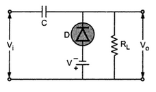
1.4 Addition of Battery in Clamper The addition of d.c.level and shape of the output can be controlled by adding additional voltage supply in series with diode with the polarity,as per the requirement. once such clamping network is shown in the Fig 10.
 |
| Fig 10 |
During first quarter of negative half cycle, when Vi becomes less than V, the diode D becomes forward biased. The capacitor gets charged instantaneously to Vm - V as shown in the Fig 11.
 |
| Fig 11 charging of capacitor |
There after capacitor retains its charge all the time and its voltage remains at Vc = Vm - V
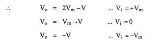
Due to this, the diode D now remains reverse biased. During positive half cycle, the circuit behaves as shown in the Fig 12.
 |
| Fig 12 positive half cycle |
Applying KVL to the circuit,

Note : Thus the d.c.shift of Vm - V gets added to the input to produce the output.
From the equation (1),
The input and output waveforms are shown in the Fig 13.
 |
| Fig 13 waveforms for clamper with d.c. source |
1.5 Clamper Application
The clamper circuits are often used in the television receivers as d.c. restorer.The video signal in television is processed through capacitively coupled amplifiers hence the signal losts its d.c.component which effectively loses black and white reference levels and the blanking level.Hence it is necessary to restore these levels back before applying signal to the picture tube. This is done by a clamper circuit acting as a d.d. restorer. This is shown in the Fig 14.
 |
| Fig 14 use of clamper circuit in television receiver |
Clamper Circuits
 Reviewed by haru
on
December 27, 2017
Rating:
Reviewed by haru
on
December 27, 2017
Rating:
Reviewed by haru
on
December 27, 2017
Rating:


No comments